


Reprogramming Blinky kits with ICSP programming
The Blinky kits each contain a microcontroller, which is a type of reprogrammable computer chip that can loaded with new code whenever you want. The chip used in each Blinky kit is the PIC16F1823 (PDF datasheet), a general-purpose 8-bit microcontroller made by Microchip.
Each chip contains two types of non-volatile memory for storing data. Here, non-volatile means that the stored data is not lost when the power is turned off. The two types of non-volatile memory are:
- Flash memory, like in a USB pocket drive, stores the main programming code in compiled form. The code is read and executed when the chip is running. The flash memory contains two separate programs: The bootloader (used for reprogramming) and the main code (reads messages from EEPROM and displays them on the LEDs). More details on the design page.
- EEPROM (Electronically-Erasable Programmable Read-Only Memory) stores the messages that are displayed on the Blinky kit’s LEDs. The “read-only” part of the name is a bit of a misnomer but is kept for historical reasons (Wikipedia has more details).
The typical use case for a Blinky kits is to use the nifty optical reprogramming system to update the messages stored in EEPROM, without changing the flash memory. If you want to change the bootloader or the main code stored in flash memory, you’ll need to use a separate process called ICSP (In-Circuit Serial Programming). ICSP requires a hardware programmer, which is typically a USB device used to interface between a computer and the flash memory inside the microcontroller. There are many different types of hardware programmers but our favorite for PIC processors is the PICkit2 (now retired) and PICkit3. They are quite reasonably priced and work great on Windows, OSX, and Linux.
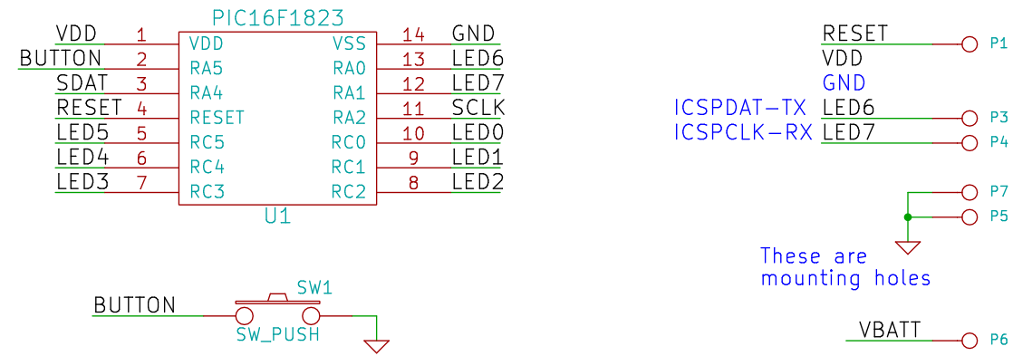
To reprogram a PIC microcontroller with an ICSP hardware programmer requires software on a computer to talk to the programmer, plus five electrical connections between the hardware programmer and the PIC chip. These electrical connections are specified in the ICSP protocol document, and are:
- MCLR / Vpp – Goes to the PIC’s reset pin. Allows the programmer to reset the chip, and provide the high voltage (Vpp) that switches the chip into flash programming mode.
- VDD – This is the chip’s normal power supply connection (usually 3-5 volts). Allows the programmer to either power the PIC itself, or to know what voltage level the PIC is being powered with externally.
- VSS – This is the chip’s normal ground (0 volt) power supply connection. The chip and the programmer need to agree on the ground reference voltage.
- ICSPDAT – Once the programmer switches the chip into flash programming mode, it sends commands and data using a two-wire protocol. This is the data pin of that two-wire protocol.
- ICSPCLK – This is the clock pin of the two-wire protocol.
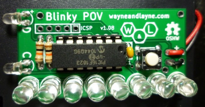
On the non-SMT Blinky kits (the Blinky Grid and Blinky POV), the ICSP signals are conveniently wired to a five-pin header row along the edge of the circuit board as shown in the image below. You can solder header pins or wires to these holes to connect your ICSP hardware programmer.
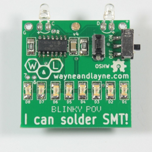
On the SMT Blinky kits (the SMT Blinky Grid and SMT Blinky POV, there wasn’t enough room to put the five pins together, but you can still reprogram the PIC chip. Option 1 is to attach test leads to the five pins on the PIC itself:
- Chip pin 4 – MCLR / Vpp (reset/programming)
- Chip pin 1 – VDD (power supply)
- Chip pin 14 – VSS (ground)
- Chip pin 13 – ICSPDAT / UART TX / LED 6 (programming data)
- Chip pin 12 – ICSPCLK / UART RX / LED 7 (programming clock)
Here’s the relevant part of the circuit schematic for reference (click to enlarge). The full schematics are available at the download page.
Option two is to solder wires into these labeled holes:
- “R” – MCLR / Vpp (reset/programming)
- “+” – VDD (power supply)
- “G” – VSS (ground)
- “6” – ICSPDAT / UART TX / LED 6 (programming data)
- “7” – ICSPCLK / UART RX / LED 7 (programming clock)
Once the five ICSP connections are made to the circuit board, use the PICkit software to program a HEX file into the chip. We have all the firmware hex files posted here on the Blinky download page.
PIC16F1823 can be replaced with PIC16F1824 or PIC16F1825 those have more FLASH and RAM.
http://www.microchip.com/wwwproducts/en/PIC16F1823
http://www.microchip.com/wwwproducts/en/PIC16F1824
http://www.microchip.com/wwwproducts/en/PIC16F1825
True, but there are some very-subtle differences between those “code compatible” chips, especially when doing weird things with flash reprogramming and bootloaders. The one I ran into most recently is that the 1823 flash memory is organized into flash erase blocks of 16 words, while the 1825 has flash erase blocks of 32 words, which changes how your bootloader operates. That being said, it’s an easy change, but still kind of annoying that those chips aren’t 100% code-compatible.