


Kicad Tutorial: PCB edges
This is part of a series of short tutorials on advanced topics of using Kicad, the favorite schematic/PCB design software here at Wayne and Layne.
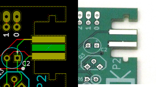
An important part of designing a PCB is to clearly indicate the outline of the board, so the board house will know how to cut your boards apart. Most PCBs are rectangular, but sometimes you want to add a more complex outline (like a circle or hexagon) or a very complex outline (like the PCB for the Video Game Shield, shown below).
To make it easier to determine where the PCB edges should be, you probably watch to switch your cursor to be the full-screen cross, by clicking the cursor toggle button in the left-most toolbar (6th down from the top).
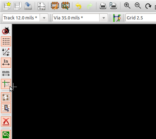
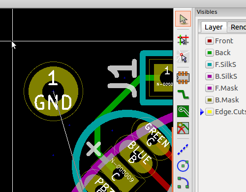
Then, select the “Edge.Cuts” layer from the list on the right side of the screen. Select the blue dashed line toolbar icon to draw graphic lines in the Edge.Cuts layer. Using the full-screen cross cursor, it is easy to find the corner of your design. Make sure to leave a little bit of clearance between the outer-most components and the PCB edge. Click to start drawing the edges, and click once in each corner of the PCB. Double-click to end the drawing.
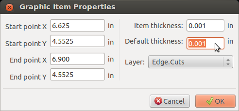
If your edge lines are not very thin, we suggest reducing their width. Right-click on each line (you might have to zoom in to ensure that your mouse cursor is pointing at the yellow line itself) and select “Edit Drawing”. Then, change the Item and Default thickness values to be 0.001″ each. We feel that this reduces confusion with the board house as to where exactly the board should be cut (“Inside of the thick line? Outside of the thick line? Middle of the thick line?” With a thin line there is no ambiguity.)
Other tutorials in this series:
Related to thiis, could you blog about how you’d do panelized boards that you can snap off after manufacture?
You might want to make a “Kicad Tutorial” category, makes it easier to share the series.
Awesome work btw.
Ken, we’ve always gotten individual boards back from the fab (we haven’t made any assembled kits yet), so we haven’t explored the panelization of PCBs.
Pat, thanks! Glad you like the tutorials! Thanks for the good suggestion, I just made a Kicad Tutorial category: http://www.wayneandlayne.com/blog/category/kicad-tutorials/
To panelize boards, from pcbnew you can use File menu -> append option to add various designs. Re-araange individual designs to form a panel (Panel dimension suiting your Fab house). Then follow usual steps of generating output gerber files for manufacturing.
@Vikas, thanks for the tip, do you have any tips on how to handle tab routing or v-scoring of the individual boards so you can separate them from the panel?
This is cool if you have calculated the coordinates for each corner beforehand. I am struggeling to modify an existing drawing, for example moving a corner. Similarly if you have a line end (not a corner), how do you grab it with the mouse and simply extend it ? This would be what I call “free drawing”. I can edit the line by calculating new start and end coordinates and changing the values, but dragging ends and corners with a mouse is far easier. I’m an ex Tango user and such tasks are incredibly easy so I find the transition tedious, but it could be me !
Another problem. I have routed a board, but need to change some track dimensions. I click on edit and get the track, but cannot change any values. I really can’t waste time with such problems. This seems in line with some comments I found which suggest that, depending on the rev you have, some functions may work, but others not. Really disappointed, but I think this is end of the road for me and KiCad.
Hi Andre,
Yep, you’re correct, there is no easy way to modify existing board outlines in pcbnew, as they appear to be independent line segments. I usually lay down by filled ground zones first, as they are easier to edit, and then draw the board outline over-top of the filled zone outline at the end. Sometimes you can adjust your grid spacing to make things easier to draw and align. Honestly I would just re-draw the board outline rather than calculate line end points.
Hi Andre,
Yep, the track dimensioning isn’t quite as WYSIWYG as anyone would like, but it’s just the way it is. I believe you might have to select the desired track thickness in the drop-down box in the upper-left, and then when you right-click a track and select “Change Track Width” or “Change Segment Width” it applies the previously-selected width to that track/segment. A bit weird at times, but seems to work ok. You can also play around with net classes, where, for example, you can set your power/ground nets to have a different thickness/clearance than other nets, that works pretty reliably.
There are always nightly builds that we help maintain (https://launchpad.net/~adamwolf/+archive/kicad-testing-daily) and are working to get nightly binaries available for all reasonable platforms. We really love working with Kicad, as the rapid development and engaging developer community are big assets, but sometimes things break and sometimes features are unfinished, left waiting for someone to pick up the ball and run with it. Sometimes free software is worth what you paid for it, but sometimes it’s totally awesome. Good luck with Kicad if you decide to try it again!
I was able to get the freerouter running on my board design and it seemed to not be able to finish the routing but Kicad’s DRC said there were no unconnected nets, 277 connects, so apparently all is well.
The autorouter is now available from Github at https://github.com/freerouting/freerouting, kindly loaded there by rusefi, I believe. It’s wonderful to have the autorouter available and many many thanks to Alfons Wirtz for the program and for Rusefi and all for making it available on Github. also thanks to Wayne and Layne for your tutorial as the instructions on freerouting are a bit confusing.
This helped me get started. I’ve written a more comprehensive guide for KiCad files to boards, specifically using OSH Park, but there are general points to.
I already have a link from there to here. A link from here to there would be much apprecuated…
http://www.arunet.co.uk/tkboyd/ele1bps.htm
Thanks for sharing the information. I am using KiCAD for couple of my PCB manufacturing.
Hi, thank for your sharing. Do you have any idea how to make the transition between two part of a line, one part is smaller than other, look smoother, like this \…./. Is this possible in KiCad?
Thanks,
Hi Khai, I am not sure what you are asking. Could you share a link to a screenshot that shows what you are asking about?
Hi All! I am a 71 year newbee to kiCad. I wonder if it is possible to make 45 degr. connection
lines i Schematic Module
Please E-mail me if anyone now howto and here as well
tj.7jmo-hbg@telia.com
Tommy Johansson in Sweden
Hi Tommy, try selecting Preferences -> General Options -> Display -> uncheck Restrict buses and wires
You may have better luck with questions here: https://forum.kicad.info/